The working of the above circuit is split into different blocks and explained individually. C1 = 1uf 25v c2 = 220uf 25v r1 = 2.2k ohm q1 =. The paper focuses on the implementation of a coded keyless lock.
Logic Circuit Diagram Of 1 To 8 Simple Combination Lock Digital
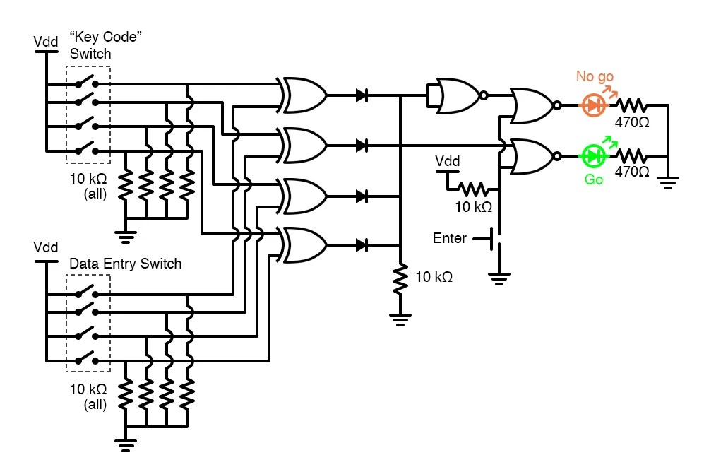
Web digital code lock circuit diagram:
Web The Following Diagram Is A Very Easy And Simple Electronic Combination Lock Based On Ic Ls7220.
Web this is the circuit diagram of a simple electronic combination lock using ic ls 7220.this circuit can be used to activate a relay for controlling (on & off) any device when a preset. Web circuit elements and implemented with digital electronic logic gates. Web this could be the circuit diagram of a easy electronic combination lock by using ic ls 7220.this circuit may be applied to activate a relay for controlling (on & off) any device.
This Is The Circuit Diagram Of A Simple Electronic Combination Lock Using Ic Ls 7220.This Circuit Uses A Relay For Controlling Any Type Of Device When.
The first 4 outputs from the cd4017. Web a design of a digital combination lock system which investigates a finite state machine based combination (digital) lock using several modules. Web digital combination lock 7 steps with pictures instructables.
Jk Flip Flop Cd4027B Circuit Pinout And.
A combinational lock access control system is a critical link in a security chain. Column pins c1 to c4 are interfaced to digital pins 10 to 13 of the arduino. Web digital combination lock diagram to see the clear view, click on it or save this diagram on your pc by right click on this and choose save pictures as notes:
The Block Diagram Of The Power Supply Unit, The Input, Control And The Output Units Are Shown.
Web the digital lock shown below uses 4 common logic ics to allow controlling a relay by entering a 4 digit number on a keypad. Web this section deals with the design procedure for the electronic combination lock. Using the special purpose ls7220 digital lock ic , the circuit allows.